starting up a new kicad project
KiCad is a suite for electronic design automation that allows the creation of both schematics and PCB for electronics projects. Over the pass 4 years of using this tool, reviewing other peoples designs within KiCad and just review more schematics I have become fairly opinionated around its use. And therfor this article will cover how to create a new kicad project and some simple first steps to take to create a good base for you to spring off of.
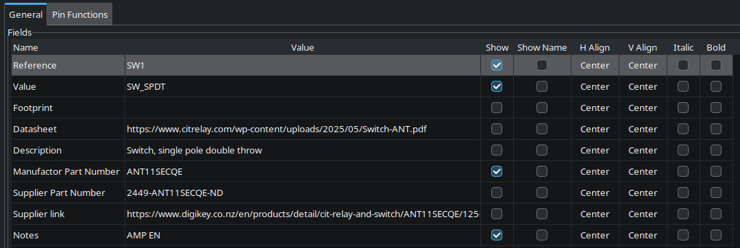
The first suggestions I have is during the start of your new project or even current project. within schematic setup (file->schematic setup) there are two different tabs I suggest you look at. “Field Name Templates” and “Net Classes”. The former allows you to add additional fields to the symbol properties, i have found it is normally very useful to add 3 fields to this:
- Supplier link : the link to where to buy the part
- Supplier Part Number : the suppliers part number for the part very often differnt from the manufacturers part number
- manufacturers part number : this is the part number itself normally KiCad libs will put this in the value field but i prefer a more explicit location for it
- Notes: this field is useful for more basic things like the voltage rating of a cap, the ppms of a resistor or the colour of an LED, things that only matter when actually selecting the part not when creating the schematic
This will then give you these additional fields when adding a new symbol.
Although during schematic creation filling these out will become tedious i prefer to fill out the notes field first just to mark down what im looking for then once the schematic is “complete” i will then proceed to actually add part numbers and links.
Luckily once this is done you can ensure that the BOM you create will have all the part required for your design.
The former suggestion being net classes this field allows for the colouring of the connections within a schematic base of the name of the net class. For my most basic project I tend to colour the nets like this
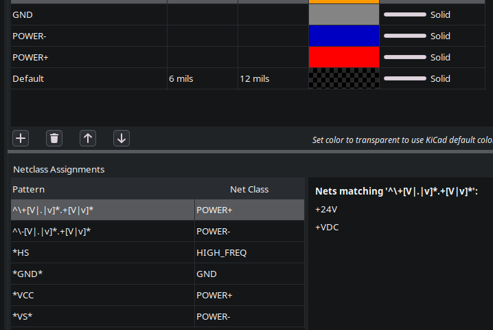
Where the positive voltages are red negative voltages are blue and gnd is a lighter grey because it shows up better on the colour theme i use. This should then allow you to easily spot where power is within your schematic and should help you with working out if something need decoupling there or not.
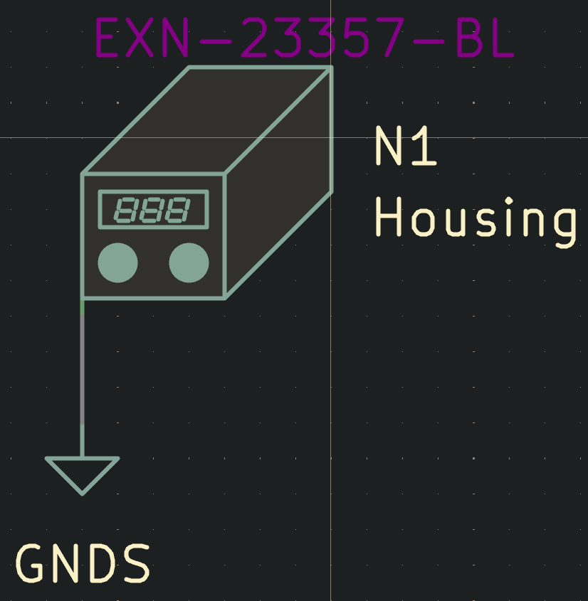
The next thing i suggest is to add a housing symbol. although i know its very likely that your project is so small it doesnt need any form of housing this is still a great symbol to think about adding, as if you do need a housing it will show up within your BOM. This is in addition to also allowing you to assign a footprint to it that contains the edge cuts and mounting holes for the thing you are mounting in
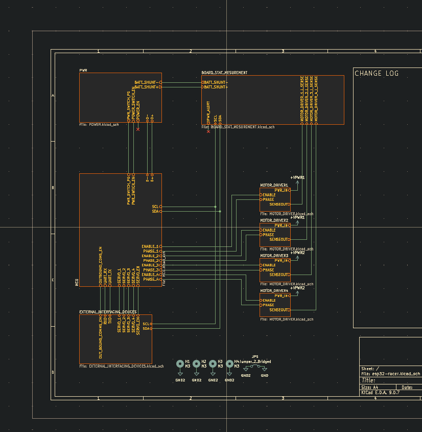
And last but not least when setting up a new KiCad project i always try to use hierarchical sheets within the design. This use of hierarchical sheets allows for you to not only think about your design within terms of functional groups but also easily show how these groups go together.